
Place of Origin:
original
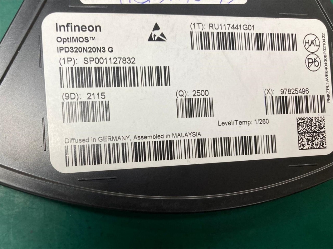
Brand Name:
INFINEON
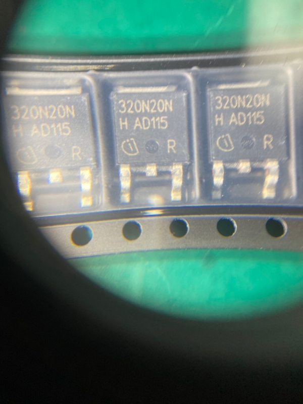
Model Number:
IPD320N20N3G
Contact Us
Application: IPD320N20N3G is an N-channel MOSFET transistor used for high-efficiency DC-DC converters and inverter applications. It can operate at high voltage, with low conduction resistance and high switching speed.
Conclusion: IPD320N20N3G has the characteristics of high efficiency, high voltage, and low conduction resistance, making it suitable for high-power DC-DC converters and inverters. It can improve the energy efficiency of the system, reduce power loss, and have a longer service life.
Parameters:
Vds (max)=200V (maximum withstand voltage)
Id=320A (maximum drain current)
Rds (on)=3.3m Ω (conduction resistance)
Qg=230nC (gate charge)
Vgs (th)=4V (gate threshold voltage)
Ciss=12300pF (input capacitance)
Coss=1170pF (output capacitance)
Crss=570pF (reverse transmission capacitance)
|
Send your inquiry directly to us

